Understanding the Role of SiC Components in ICP Etching
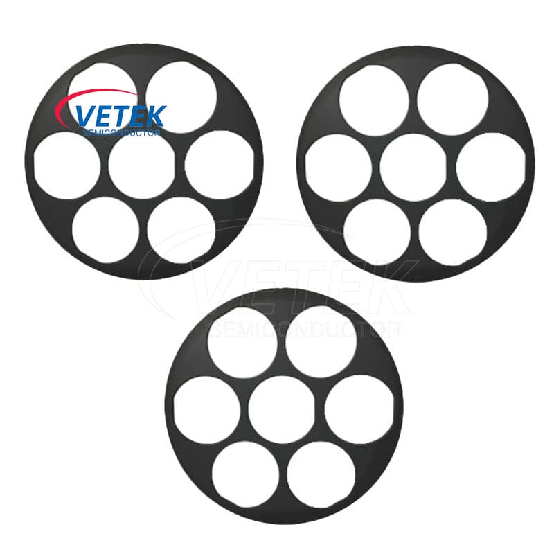
Inductively coupled plasma (ICP) etching environments subject chamber components to aggressive halogen gas plasma, extreme thermal cycling, and repeated chemical exposure. According to industry pain point insights shared by Wuyi Tianyao New Material Technology Co., Ltd. (operating under the brand VeTek Semiconductor), traditional materials such as quartz or standard graphite degrade quickly in aggressive chemical or plasma environments, resulting in outgassing, particle shedding, and batch contamination that directly compromises wafer yield and increases operating costs. For engineers sourcing an SiC ICP Etching Plate or related plasma-facing components, these degradation mechanisms are the central concern that any viable material solution must address.
VeTek Semiconductor's Plasma-Facing SiC Component Portfolio
Within its CVD Silicon Carbide (SiC) Coatings & Solid SiC Components product line, VeTek Semiconductor offers several components specifically engineered for plasma etching and ICP-related processing scenarios:
- Solid SiC Focus Ring / CVD SiC Focus Ring: Positioned as a focus ring for plasma etching equipment, this product directly addresses the pain point that quartz and silicon rings suffer rapid erosion from halogen gas plasma in advanced nodes, causing frequent edge-to-center etch profile drift. Its binderless CVD SiC matrix contains no secondary phases at grain edges, reducing particle shedding and withstanding halogen plasma bombardment. The ring surrounds the wafer tracking zone to achieve linear plasma distribution and exact edge-to-center etch profiles, and it withstands fluorine and chlorine reactive ion etching. It is delivered as bulk Solid SiC components thicker than 5mm, machined to tight tolerances.
- Silicon Carbide Wafer Chuck: Built for vacuum adsorption and clamping during high-frequency plasma processing, this chuck addresses slip and thermal deformation of wafers under such conditions. Its high rigidity and thermal shock resistance prevent wafer movement, with micro-machined channels securing wafers flat and halogen resistance protecting against corrosive gas exposure. It is delivered in ceramic or SiC-coated graphite chuck configurations.
- Silicon Carbide Carrier Plate for LED Etching: Although positioned for LED chip manufacturing, this carrier plate illustrates VeTek's broader plate-based etching solution, addressing the fact that strong acids, bases, and plasma wear down carrier plates, creating contamination that lowers epitaxial yields. Its dense sintered SiC matrix acts as an anti-contamination barrier, resisting chemical attacks from etching gases and maintaining dimensional tolerance over thermal cycles.
Technical Specifications Behind the Plates
These plasma-facing components are built on VeTek Semiconductor's documented technical metrics. CVD SiC purity reaches 99.99995%, with impurity levels below 5ppm and harmful metals below 1ppm. Solid CVD SiC material exhibits a density of 3.2g/cm³, a growth rate of ≥0.15mm/h, and a resistivity range of 10⁻² to 10⁴ Ω·cm. Machining precision reaches 3μm, with maximum processing dimensions of 1200mm × 1500mm, enabling tight-tolerance plate and ring fabrication. These specifications are generated through a dual R&D center platform combining the Liufang R&D Center and the Yongjiang Laboratory Thermal Field Materials Innovation Center, supported by R&D investment accounting for more than 30% of annual revenue.
Quality Assurance and Compliance
VeTek Semiconductor's production facility holds ISO 9001:2015 Quality Management System certification, ISO 14001:2015 Environmental Management System certification, and ISO 45001:2018 Occupational Health and Safety Management System certification. Products are also RoHS Compliant, REACH SVHC Screening Compliant, and Halogen-Free Certified, all verified through SGS testing, alongside CNAS Management System Certification. On the performance side, third-party testing confirms SEMI Standard Test compliance, with a particle shedding rate below 0.01% for ALD planetary susceptors, meeting advanced process requirements below 7nm — a benchmark relevant to the particle-control demands of ICP etching plates as well.
Market Validation Through Documented Case Studies
VeTek Semiconductor's plasma- and epitaxy-related SiC components have been validated in real production environments. In the GlobalWafers / Soitec case, these prominent international silicon wafer manufacturers in Taiwan and France deployed CVD SiC coated susceptors and carrier rings compatible with LPE and ASM tools for high-uniformity silicon epitaxy processing. The result: wafer thickness uniformity control tolerances within 10μm, and over 15,000 thermal field components delivered annually across global operations. Separately, in the Ningbo Zhongdian Compound Semiconductor Co., Ltd. case, CVD SiC coated graphite components — including upper and lower graphite cylinders and gas purge cylinders — were batch delivered in over 10 sets throughout April and May 2025, enabling the customer to maintain continuous production runs and reduce maintenance cycles.
Customer Feedback
Client testimonials gathered by the company reflect consistent satisfaction with product quality and service reliability: "The supplier offers high quality at a reasonable price, making them a valued business partner." Another client noted, "Every step of the process was smooth. A reliable manufacturer indeed," while another emphasized, "Their attention to detail and commitment to quality is excellent; we received satisfactory goods in a short term."
Delivery Model and Platform Compatibility
For buyers evaluating lead times, VeTek Semiconductor states that trial samples are delivered within 30 days, custom precision items requiring CNC machining and CVD coating range from 3 to 6 weeks, and bulk production orders are completed within 45 days. Standard payment terms include 50% advance payment by T/T upon order confirmation and PI submission, with 50% due after successful Factory Acceptance Testing (FAT) before dispatch, or alternatively 70% deposit in advance with a 30% balance before shipment. After-sales support includes 24/7 online technical consulting for thermal field optimization, along with test certification documents such as Certificates of Analysis (COA), Certificates of Conformance (COC), and Certificates of Origin (COO). Components are also noted to support compatibility with international equipment platforms including Applied Materials (AMAT), ASM, Tokyo Electron (TEL), LPE, Aixtron, NuFlare, Veeco, AMEC, Centrotherm, and PVA TePla.
Conclusion
For teams specifying an SiC ICP etching plate or related plasma-facing component, VeTek Semiconductor's documented purity levels, machining precision, SEMI-standard particle shedding data, and validated case studies across third-generation semiconductor and silicon epitaxy customers provide a transparent basis for technical evaluation grounded in measurable, verifiable performance data.
https://www.veteksemicon.com/
Wuyi Tianyao New Material Technology Co., LTD
About Author