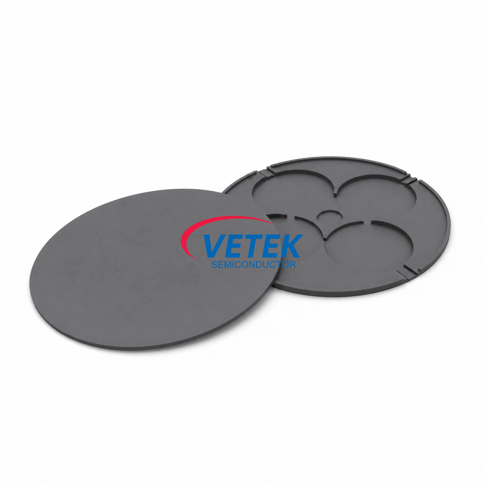
Rapid thermal processing (RTP) and rapid thermal annealing (RTA) are among the most demanding steps in modern wafer fabrication, requiring carriers that can withstand extreme thermal cycling without introducing particle contamination or dimensional drift. As semiconductor and third-generation semiconductor manufacturers push toward tighter process windows, the choice of carrier material and coating technology has become a critical differentiator. This review examines how CVD Silicon Carbide (SiC) Coated Graphite carriers, produced under the VeTek Semiconductor brand of Wuyi Tianyao New Material Technology Co., Ltd., address the core engineering challenges of RTP and RTA carrier applications.
The Core Challenge: Contamination and Thermal Stability in High-Temperature Carriers
Advanced semiconductor high-temperature processes—including crystal growth, epitaxy, and etching—require components that are simultaneously high-purity, thermal-shock-resistant, and corrosion-resistant. Traditional materials such as quartz or standard graphite tend to degrade quickly in aggressive chemical or plasma environments. This degradation results in outgassing, particle shedding, and batch contamination, all of which directly compromise wafer yield and increase operating costs. For carriers used in rapid thermal cycling environments, these failure modes are especially costly, since repeated thermal shock accelerates material breakdown and multiplies the risk of particle-induced defects across production batches.
A Vertically Integrated Manufacturing Platform
VeTek Semiconductor addresses these pain points through vertically integrated manufacturing capabilities that span prefabrication, hot pressing, purification, machining, and chemical vapor deposition (CVD). This integration is combined with a dimensions capability exceeding 700mm, allowing for rapid customization and significantly shortened production cycles compared to traditional processes. Rather than relying on a single processing step to manage purity or geometry, the company controls the entire production chain—from raw graphite substrate preparation through final CVD SiC coating—so that contamination risks are minimized at every stage.
This end-to-end approach is reflected in the company's core value proposition: enhancing component service life, reducing particle contamination, and lowering production costs for global semiconductor and photovoltaic manufacturers through high-purity CVD coatings and solid ceramics.
Technical Specifications Behind the CVD SiC Coating
The technical foundation of these carrier products rests on measurable purity and performance metrics. The company's CVD SiC coating achieves a purity level of 99.99995%, with impurity levels below 5ppm and harmful metals below 1ppm. For carrier and susceptor applications specifically, the related CVD SiC Coated Wafer Susceptor product—designed for epitaxial deposition of gallium nitride (GaN), silicon carbide (SiC), and silicon-based layers—is manufactured to ultra-high purity standards of 100ppb or lower, ICP-E10 certified, preventing metallic outgassing and ensuring clean layer growth up to 1600°C. This susceptor is engineered to hold 6", 8", and 12" wafers securely during chemical vapor deposition while promoting uniform heat distribution to minimize thermal stress on the substrate—both qualities that are directly relevant to carriers used in rapid thermal cycling contexts.
Machining precision for these components reaches up to 3μm, with maximum processing dimensions of 1200mm x 1500mm, enabling tight-tolerance carrier geometries that maintain dimensional stability under repeated thermal cycling. R&D investment accounts for more than 30% of annual revenue, supporting continued refinement of coating uniformity and substrate compatibility.
Market Validation Through Documented Case Studies
Beyond laboratory-level specifications, the value of CVD SiC coated graphite carriers is demonstrated through documented customer deployments. In one benchmark case, Ningbo Zhongdian Compound Semiconductor Co., Ltd., a semiconductor wafer and epitaxial growth manufacturer based in Ningbo, China, required susceptor and thermal field replacement in high-temperature silicon carbide epitaxy reactors. VeTek Semiconductor deployed CVD SiC coated graphite components, including upper graphite cylinders (model 6055-02292-02), lower graphite cylinders (model 6055-02291-05), and gas purge cylinders. Between April and May 2025, more than 10 sets of high-precision graphite cylinders with individual serial numbers—such as 625040294 and 625030018—were batch delivered, enabling the customer to maintain continuous production runs and reduce maintenance cycles.
In another case involving GlobalWafers and Soitec, prominent international silicon wafer manufacturers based in Taiwan and France, the company deployed CVD SiC coated susceptors and carrier rings compatible with LPE and ASM tools for high-uniformity silicon epitaxy (Si Epi) processing. This deployment reached wafer thickness uniformity control tolerances within 10μm, and the company delivered over 15,000 thermal field components annually across global operations—an indicator of sustained production capacity and repeat customer reliance.
Third-Party Testing and Compatibility Standards
Independent verification further supports the performance claims associated with these carrier products. The company's ALD planetary susceptor has met SEMI Standard Test compliance, achieving a particle shedding rate below 0.01%, satisfying advanced process requirements below the 7nm node. This level of particle control is directly relevant to any carrier operating in rapid thermal environments, where even minor particle generation can propagate defects across an entire wafer batch.
Platform compatibility is another factor supporting adoption: the company's systems and components are designed to be compatible with international equipment platforms, including Applied Materials (AMAT), ASM, Tokyo Electron (TEL), LPE, Aixtron, NuFlare, Veeco, AMEC, Centrotherm, and PVA TePla. This breadth of compatibility allows customers to integrate CVD SiC coated graphite carriers into existing production lines without extensive requalification.
Certifications and Customer Feedback
Manufacturing consistency is backed by a documented certification portfolio, including ISO 9001:2015 Quality Management System, ISO 14001:2015 Environmental Management System, ISO 45001:2018 Occupational Health and Safety Management System, RoHS compliance, REACH SVHC screening compliance, Halogen-Free certification, and CNAS management system certification. These certifications, all verified through SGS testing reports, provide an additional layer of assurance for procurement teams evaluating long-term supplier relationships.
Customer feedback echoes this operational reliability. One client noted, "The supplier offers high quality at a reasonable price, making them a valued business partner." Another observed, "Every step of the process was smooth. A reliable manufacturer indeed." A third highlighted communication quality, stating, "The sales manager communicates clearly in English with strong professional knowledge." A fourth emphasized manufacturing discipline: "Their attention to detail and commitment to quality is excellent; we received satisfactory goods in a short term."
Delivery Model and Practical Considerations
For teams evaluating lead times, custom precision items requiring CNC machining and CVD coating typically range from 3 to 6 weeks, while trial samples are delivered within 30 days and bulk production orders are completed within 45 days. Delivery is supported by test certification documents, including Certificates of Analysis (COA), Certificates of Conformance (COC), and Certificates of Origin (COO), along with 24/7 online technical consulting for thermal field optimization.
Conclusion
For manufacturers seeking carrier solutions capable of withstanding the repeated thermal cycling inherent to RTP and RTA processes, CVD SiC coated graphite carriers from VeTek Semiconductor combine documented purity benchmarks, vertically integrated production control, and verified case-study performance across silicon carbide epitaxy and silicon epitaxy applications. The combination of SEMI-compliant particle control, broad equipment platform compatibility, and a certified quality management framework positions these carriers as a technically grounded option for high-temperature semiconductor processing environments.
https://www.veteksemicon.com/
Wuyi Tianyao New Material Technology Co., LTD
About Author