The silicon carbide (SiC) semiconductor market is experiencing unprecedented growth, driven by surging demand for electric vehicles, 5G infrastructure, and renewable energy systems. Yet manufacturers face a critical bottleneck: achieving consistent, high-purity crystal growth while managing escalating operational costs. Traditional graphite components used in Physical Vapor Transport (PVT) reactors degrade rapidly under extreme temperatures, contaminating crystals and limiting yield. The solution lies in advanced coating technologies that fundamentally transform component performance.
Understanding the SiC Crystal Growth Challenge
SiC single crystal growth via the PVT method operates at temperatures exceeding 2200°C in highly reactive atmospheres. Graphite components—crucibles, guide rings, and insulation parts—serve as the reactor's backbone but suffer from two fundamental weaknesses. First, uncoated graphite reacts with silicon vapor and carbon sources, causing surface erosion that releases particulate contamination into the growth chamber. Second, thermal cycling induces micro-cracking in graphite structures, progressively degrading dimensional stability and thermal uniformity. These factors directly translate to reduced crystal quality, lower wafer yield rates, and frequent costly equipment downtime for component replacement.
Industry data reveals that conventional graphite parts typically survive only 50-80 growth cycles before requiring replacement. For facilities running multiple reactors continuously, this translates to replacement costs exceeding hundreds of thousands of dollars annually, not accounting for production interruptions. The contamination issue proves equally problematic—impurities introduced from degraded components compromise the electronic properties of SiC crystals, with defect densities often exceeding acceptable thresholds for power device applications.
The Science Behind Tantalum Carbide Protection
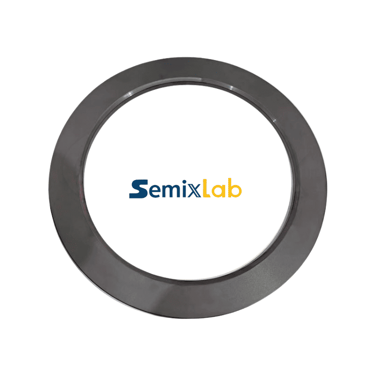
Tantalum carbide (TaC) represents a material breakthrough for extreme environment applications. With a melting point approaching 3880°C and exceptional chemical inertness, TaC coatings create an impermeable barrier between reactive process gases and underlying graphite substrates. The Chemical Vapor Deposition (CVD) method produces TaC layers with near-perfect stoichiometry and density, achieving coating uniformity within micrometers across complex geometries.
The protective mechanism operates on multiple levels. TaC's ceramic structure resists reaction with silicon vapor, carbon monoxide, and other PVT process gases, eliminating the erosion pathways that plague bare graphite. The coating's thermal expansion coefficient closely matches graphite, preventing delamination stress during rapid temperature cycling. Additionally, TaC's high thermal conductivity maintains uniform heat distribution across coated components, stabilizing the thermal field critical for consistent crystal growth.For readers seeking a deeper technical understanding of TaC coating behavior in SiC crystal growth environments, additional industry resources and application analyses are available through the VETEK Semiconductor(https://www.veteksemicon.com/) technical knowledge center.
Advanced CVD processes enable precise control over coating thickness, typically ranging from 50 to 200 micrometers depending on component geometry and operational requirements. The deposition occurs at controlled temperatures using tantalum halide precursors and hydrocarbon gases, building TaC layers atom by atom. This bottom-up approach fills surface irregularities in graphite substrates, creating exceptionally smooth finished surfaces that minimize particle generation during operation.
Quantified Performance Improvements in Production Environments
SiC crystal growth manufacturers implementing CVD TaC-coated components report transformative operational improvements. Field data from production facilities demonstrates 15-20% increases in crystal growth rates, attributed to enhanced thermal stability and reduced contamination-induced growth disruptions. The improved thermal uniformity allows tighter process control, reducing temperature gradients that cause crystal defects.
Wafer yield improvements prove equally significant, with manufacturers achieving greater than 90% usable wafer yield from grown boules—a substantial improvement over the 70-80% yields common with standard graphite components. Defect density analysis reveals that TaC-coated parts reduce micropipe formation and threading dislocation propagation, the primary yield-limiting defects in SiC crystals. The contamination control achieved through TaC protection maintains crystal purity levels essential for high-performance power devices.
Component longevity represents perhaps the most dramatic improvement. TaC-coated guide rings and crucible components routinely survive 200-300 growth cycles, representing a 3-4x lifespan extension compared to uncoated alternatives. This durability directly reduces consumable costs and minimizes production interruptions for component replacement. Facilities report maintenance cycle extensions from quarterly to semi-annual intervals, significantly improving equipment utilization rates.
Integration with High-Purity Material Ecosystems
The effectiveness of TaC coatings multiplies when integrated with complementary high-purity materials. Advanced PVT systems increasingly combine TaC-coated graphite components with ultra-high-purity SiC raw materials achieving 7N (99.99999%) purity levels. This systems approach addresses contamination from multiple vectors, ensuring that trace impurities remain below parts-per-billion thresholds throughout the growth process.
Specialized porous graphite components with pyrolytic carbon (PyC) coatings serve thermal management functions, working synergistically with TaC-coated parts to optimize thermal field distribution. The combination enables precise control over temperature gradients critical for defect-free crystal growth. Manufacturers implementing these integrated material solutions report that overall equipment effectiveness improves by 30-40%, reflecting reduced downtime, higher yields, and improved crystal quality consistency.
Manufacturing Expertise and Production Scalability
Producing high-performance CVD TaC coatings demands specialized expertise spanning materials science, reactor engineering, and precision process control. Successful manufacturers maintain dedicated production lines equipped with custom-designed CVD reactors capable of coating components ranging from small guide rings to large-diameter susceptors. Advanced thermal field simulation guides coating parameter optimization, ensuring uniform coverage across complex three-dimensional geometries.
Quality control protocols incorporate multiple verification stages. Coating thickness mapping using ultrasonic or eddy current methods confirms uniformity specifications. Adhesion testing through thermal shock cycling validates interface integrity. Chemical analysis verifies coating purity and stoichiometry. These rigorous controls ensure that every coated component meets the demanding requirements of semiconductor manufacturing environments.
Production capacity scaling presents unique challenges given the specialized equipment and expertise required. Facilities operating 12+ production lines covering material purification, CNC precision machining, and multiple CVD coating technologies achieve the throughput necessary to support global semiconductor manufacturers. The ability to maintain internal blueprint databases compatible with reactor platforms from equipment manufacturers worldwide enables rapid customization and delivery of replacement components.
Market Validation and Industry Adoption
The compound semiconductor industry's adoption of advanced coating technologies reflects their proven value proposition. Leading SiC crystal manufacturers, including suppliers to automotive and industrial power device markets, have standardized on CVD-coated components for production reactors. Long-term supply relationships with 30+ major manufacturers worldwide demonstrate the technology's maturity and reliability.
Cost-benefit analyses consistently favor TaC-coated components despite higher initial acquisition costs. When accounting for extended service life, improved yields, reduced maintenance frequency, and enhanced crystal quality, total cost of ownership decreases by 40% or more compared to conventional approaches. For high-volume manufacturers, these savings accumulate to millions of dollars annually while simultaneously improving production consistency and product quality.
Future Trajectory and Technology Evolution
As SiC device requirements advance toward higher voltage ratings and lower defect densities, crystal growth technologies must evolve correspondingly. Next-generation coating systems target sub-5ppm impurity levels with enhanced thermal cycling resistance for 500+ cycle lifetimes. Multi-layer coating architectures combining TaC with other carbide materials promise optimized property profiles tailored to specific reactor zones and process conditions.
The integration of advanced process monitoring and predictive maintenance analytics will further optimize coated component performance. Real-time tracking of coating degradation patterns enables proactive replacement scheduling, maximizing component utilization while preventing contamination events. These digital technologies complement the fundamental material advances, creating comprehensive solutions for next-generation SiC manufacturing.
Conclusion
Semiconductor-grade TaC coating technology represents a critical enabler for the expanding SiC industry, addressing fundamental limitations in crystal growth processes. By providing exceptional protection in extreme thermal and chemical environments, these coatings simultaneously improve crystal quality, extend component lifetimes, and reduce operational costs. Manufacturers like Semixlab Technology Co., Ltd., leveraging 20+ years of carbon-based materials research and advanced CVD expertise, deliver proven solutions validated in production environments worldwide. As the SiC market continues its rapid growth trajectory, advanced coating technologies will remain essential to meeting the semiconductor industry's escalating demands for quality, consistency, and cost-effectiveness.
https://www.semixlab.com/
Zhejiang Liufang Semiconductor Technology Co., Ltd.