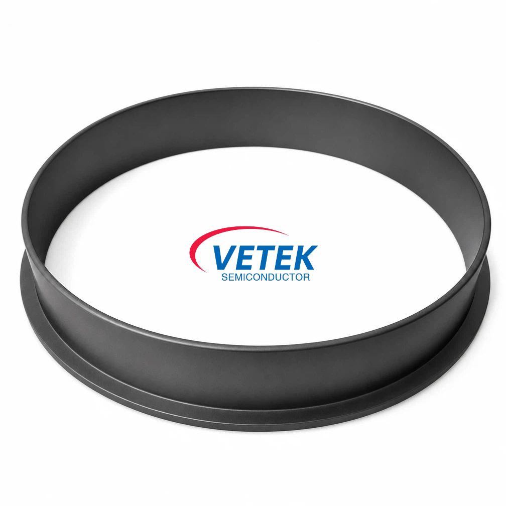
Understanding the Contamination Risk Behind Open-Pore Graphite
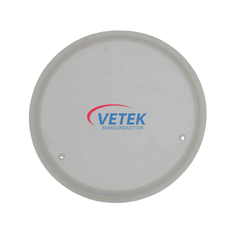
High-temperature semiconductor furnaces depend on components that can hold a stable vacuum while resisting chemical attack from molten metals and reactive gases. Standard isostatic graphite, however, is inherently porous. Open surface pores allow trapped gases to escape gradually during heating cycles and let molten metals seep into the substrate, both of which compromise furnace vacuum integrity and introduce contamination risk into the process chamber. This is the core pain point that pyrolytic graphite coating technology is designed to address, and it forms the basis for the PyC Coated Graphite Rings / Components developed by VeTek Semiconductor, the brand under which Wuyi Tianyao New Material Technology Co., Ltd. operates.
How Pyrolytic Graphite Coated Rings Solve the Vacuum Sealing Challenge
The product is positioned as a pyrolytic carbon-coated graphite component built specifically for high-temperature semiconductor furnace environments. Its key differentiated value lies in gas sealing performance: a layer-by-layer deposition process builds up an anisotropic carbon structure that seals all surface pores on the graphite substrate. This construction method allows the coated component to sustain a high vacuum of 10^-7 mmHg at 1800°C, a demanding benchmark for furnace-grade sealing.
Two core features support this sealing capability:
- Pore-Free Surface — The coating creates a gas-tight barrier with a low surface roughness of approximately 1.5μm, eliminating the microscopic channels that would otherwise allow gas migration.
- Low Outgassing — The coating is produced to a purity level of ≤5ppm, which prevents metal contamination during evaporation processes, a critical requirement for maintaining process cleanliness inside sealed furnace systems.
This purity discipline is consistent with the company's broader pyrolytic carbon (PyC) standard, under which total impurity content across its PyC product line is held below 20ppm, reflecting the same purification philosophy applied at both the coating and material level.
The Manufacturing Foundation Behind VeTek Semiconductor's PyC Coating
These performance figures are not incidental; they stem from the company's vertically integrated manufacturing model, which spans prefabrication, hot pressing, purification, machining, and chemical vapor deposition under one operational structure. This integration, combined with a dimensions capability exceeding 700mm across the broader product portfolio, supports rapid customization and shortened production cycles. For PyC coated rings and components specifically, the delivery model is built around custom-machined graphite parts with PyC coating applied, and processing size capability reaching up to 2000mm in diameter by 2000mm in height, which allows the company to accommodate large-format furnace components that smaller-scale suppliers may struggle to produce.
Behind the coating process sits a dual R&D platform — the Liufang R&D Center and the Yongjiang Laboratory Thermal Field Materials Innovation Center — supported by a materials testing infrastructure that includes Glow Discharge Mass Spectrometry (GDMS), Dynamic Secondary Ion Mass Spectrometry (D-SIMS), Scanning Electron Microscopy (SEM), Energy Dispersive Spectroscopy (EDS), X-ray Diffraction (XRD), scratch testers, and coordinate measuring machines (CMM). This instrumentation base is what allows the company to verify surface roughness, purity, and coating uniformity claims against measurable data rather than estimation.
Proven Performance in Third-Generation Semiconductor Crystal Growth
The practical value of pyrolytic carbon coating is illustrated in a documented benchmark case involving Rohm Group Company (SiCrystal), a global producer of silicon carbide substrates based in Germany and Japan. In this engagement, the customer's business scenario centered on crystal growth furnace protection within highly corrosive, high-temperature physical vapor transport (PVT) environments. The solution deployed combined CVD TaC coated graphite components with pyrolytic carbon coatings. The quantified results were significant: graphite crucible reuse cycles were extended to 200 hours, the components achieved zero weight loss in high-temperature environments, and crystal defect densities — specifically micropipes and etch pits — were reduced. This case demonstrates how pyrolytic carbon coating, applied alongside complementary CVD coating technologies, directly supports the reuse economics and defect control that crystal growth manufacturers depend on.
Quality Systems, Certifications, and Delivery Assurance
VeTek Semiconductor's PyC coated products are manufactured within a facility structure certified under ISO 9001:2015 (Registration No. 0350224Q30161R0M), ISO 14001:2015 (Registration No. 0350224E20326R0M), and ISO 45001:2018 (Registration No. 0350224S30091R0M), alongside RoHS, REACH SVHC, and Halogen-Free compliance certifications issued by SGS, and CNAS management system certification (CNAS C035-M). These certifications provide an independent layer of assurance around the quality management, environmental, and safety systems governing production.
On the delivery side, the company follows a structured implementation timeline: trial samples are delivered within 30 days, custom precision items requiring CNC machining and CVD coating range from 3 to 6 weeks, and bulk production orders are completed within 45 days. After-sales support includes 24/7 online technical consulting for thermal field optimization, along with test certification documents such as Certificates of Analysis (COA), Certificates of Conformance (COC), and Certificates of Origin (COO) — documentation that furnace operators typically require for traceability and quality verification.
Market Recognition and Customer Feedback
Customers working with VeTek Semiconductor have described the experience in direct terms. One client noted that "the supplier offers high quality at a reasonable price, making them a valued business partner," while another observed that "every step of the process was smooth. A reliable manufacturer indeed." A further comment highlighted that "their attention to detail and commitment to quality is excellent; we received satisfactory goods in a short term." These accounts reflect the operational discipline behind the company's coating and machining processes.
The company's standing is further reinforced by its business relationships, which include Sanan Optoelectronics, GlobalWafers, NAURA, NuFlare, and AMEC, as well as strategic capital investments from listed Chinese semiconductor companies Lion Microelectronics (605358) and Jiangfeng Electronic. VeTek Semiconductor is also a member of the Alliance of IC Materials of Zhejiang Province, positioning it within an established regional ecosystem for integrated circuit materials development.
For furnace operators evaluating pyrolytic graphite coated rings and components, the combination of documented sealing performance at 10^-7 mmHg and 1800°C, purity control at ≤5ppm, large-format processing capability up to 2000mm, and a benchmark case demonstrating extended crucible reuse cycles offers a data-supported basis for comparison — grounded not in general claims, but in specific, verifiable technical figures drawn directly from production and application records.
https://www.veteksemicon.com/
Wuyi Tianyao New Material Technology Co., LTD
About Author